![]()
 ANDOR DESIGN CORP
![]()
ANDOR DESIGN CORP
|
|
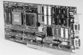
CIC429
8 CHANNELS ARINC 429
Simulator Analyzer Tester
5/8 size ISA Bus Interface Card
AVIONICS BUSES SUPPORTED
ARINC 429, 571, 575, 706 or similar buses
FEATURES
* 5/8 SIZE PC CARD.
* 8 INDEPENDENT CHANNELS.
* PROGRAMMABLE ERROR INJECTION.
* PROGRAMMABLE WORD GAP.
* MULTIPLE OR CONTINUOUS TRANSMISSIONS.
* PERIODIC/APERIODIC MESSAGE SCHEDULING
* 256 KBYTE DUAL PORT, FAST, STATIC RAM.
* 24 BITS TIME TAG.
* ON BOARD MICROPROCESSOR.
DESCRIPTION
The CIC429 is a full
featured, high performance Serial bus Simulator Analyzer Tester developed by
Andor Design for test and simulation of ARINC 429 or similar Avionic buses. The
CIC429 is designed as a 5/8 size plug-in card for an ISA bus.
An on board microprocessor
off loads the host by organizing the data in a predefined structure in the dual
port RAM. Programming the CIC429 consists of changing this data, which can be
done on the fly for real time applications.
The CIC429 features four independent transmit and four independent
receive channels. Each channel can be programmed for either 32 or 25-bit data
format and high or low data rate.
Each transmit channel
provides a message scheduler for
periodic or aperiodic and single or continuous transmission. Transmit
messages are programmable for parity, error injection and gap setting. The
input to each receive channel can be selected from its own bus or any of the
four output channels. Received data words are filtered, time tagged, annotated
with a breakdown of detected errors and stored under program control in a
circular buffer. The user may define additional circular buffers for each
Channel Label and SDI bits.
|
|
|
|
|
|
|
ISA BUS ARINC
DATA ARINC ARINC INTERFACE
Channels Selectors Buffers BUSSES ┌───────────┐ ┌───────┐ ┌──────────┐
│ Dual Port │ │───>│Tsmt
1 │─────────────>│──────>│Driver
1 │───>
Tsmt BUS 1 ISA Bus <──>│
SRAM │<─>│ ├───────┤ │ ├──────────┤ │ │ │───>│Tsmt
2 │─────────────>│──────>│Driver
2 │───>
Tsmt BUS 2 └───────────┘ │ ├───────┤ │ ├──────────┤ ┌───────────┐ │───>│Tsmt
3 │─────────────>│──────>│Driver
3 │───>
Tsmt BUS 3 Ext
Strt
────>│ Micro │<─>│
├───────┤ │
├──────────┤ │ Processor
│
│───>│Tsmt 4
│─────────────>│──────>│Driver
4 │───? Tsmt
BUS 4
└───────────┘ │ └───────┘ │
└─┬────────┘ Ampl
────────────────────────┼───────────────────────────┼─────────┘ │
└────┐ │
┌───────┐ ┌────────┐<──│
┌──────────┐
│<───│RCV 1 │<─────│ Mux 1
│<──┼──│Receiver
1│<─── Rcv BUS 1
┌──────────┐ │ ├───────┤
├────────┤<──│ ├──────────┤ │ Time Tag
│<─>│<───│Rcv 2
│<─────│ Mux 2
│<──┼──│Receiver
2│<─── Rcv BUS 2
└──────────┘ │
├───────┤ ├────────┤<──│
├──────────┤
│<───│Rcv 3 │<─────│ Mux 3
│<──┼──│Receiver
3│<─── Rcv BUS 3
┌─────────┐ │ ├───────┤
├────────┤<──│ ├──────────┤ │ Oscill │
│<───│Rcv 4 │<─────│ Mux 4 │<──┼──│Receiver
4│<─── Rcv BUS 4 └─────────┘ └───────┘ └────────┘ └──┬───────┘ Thresh
────────────────────────────────────────────────────────────┘ |
- Word Length 32 or 25 Bits
- Data Rate 100 or 12.5
Kilo Bits per sec
- Parity Even,
Odd, None
- Filtering Per Label
& SDI
- Word Gap 2 to 65536
Null Bits
- Minor Frame 16 bits, 80
micro sec. Res.
- Amplitude Adjust 2 to 10
Volts A to B
- Threshold Adjust 0 to
7 Volts A to B
- External Starts 5
Volts TTL Pulses
ERROR INJECTION/REPORTING
‑ Parity
‑ Encoding
‑ High bit count
- Low bit count / Gap
|
M A X I M U M |
R A T I N G S |
|
Parameter |
Value |
|
Temperature Range Operating Storage Power supplies Logic +5 Volts +/‑ 5% +12 Volts +/‑ 5% -12 Volts +/‑ 5% Physical
characteristics |
0 to
+70 Deg. C ‑65 to +150
Deg. C .350 Amps
Max. .035 Amps Max. .035 amps Max. 4.4 x 8.4 x 0.44 inches |
The CIC429 comes with
software libraries, drivers and assorted utilities for DOS, Windows and Windows
NT. Source code written in "C" is included.
A menu driven user
interface is included for stand alone operation. With this program the user can
schedule and initiate ARINC messages on the transmit channels. He can receive
and monitor all or selected ARINC traffic in real time.
- I/O channel address
- Interrupt level
- Rise/Fall time
TRANSMIT OPERATION
The user writes a set of
Command Blocks, a message list and number of messages to define a Minor Frame.
He writes a Minor Frame time, the number of Minor Frames per Major Frame and a
Minor Frame list to define a Major Frame. The Major and Minor frames define the
periodic / aperiodic message schedule.
The transmitter sends the Major Frame a number of times as programmed in
the Major Frame count, without any further attention from the CPU.
The user writes a set of
Command Blocks and a filtering table to capture incoming messages. Filtering is
defined for each channel per Label and SDI bits. Captured messages are time
tagged, annotated with the channel number and a breakdown of any detected
errors and saved in the static RAM. An interrupt can be enabled on selected
messages.
Buffers are assigned by the
user for messages of interest per
Channel, Label and SDI combinations. An additional dedicated buffer is
shared by all messages. Both buffers are circular, the size of the first is
user defined. Messages can be stored in either or both under program control.
The CIC429 will normally
return an I/O channel ready to the CPU in 50 to 100 nanoseconds. This time is
extendible to 900 nanoseconds if the CIC429 is accessing the dual port RAM.
The CIC429 operates as a
16-bit I/O channel slave device. It generates interrupt flags to show
completion of a frame, receipt of a specified Label and SDI Bits, detected
message errors or triggers.
A dual ported, I/O mapped,
static RAM serves as the intermediate for data exchange with the ARINC bus. An
auto incrementing address register serves to hold the initial RAM address while
a single I/O address serves for data transfer. Both the register and the RAM
can be loaded with new data while a message is being transmitted over the ARINC
channel.
For specialized features or unique interface requirements, please
contact the factory.
Specifications subject to change without notice.
Copyright (c) 1997 – 2007 by Andor Design Corp.
All rights reserved.
ANDOR DESIGN CORP. www.AndorDesign.com
20 Pond View Drive Telephone
516 364 1619
Syosset, New York, USA 11791-4409 FAX 516
364 5428
Data
Sheet, Jan 15, 1997